Intel, arguably the household name in personal computers, has lagged rivals in chip transistor densities – some say by as much as two years – in recent times, and performance of its chips are behind competitors.
Still, the chipmaker is keen to highlight its competitive differentiation in areas like semiconductor sorting and packaging, and plans to reclaim process leadership by 2025 remain well on track.
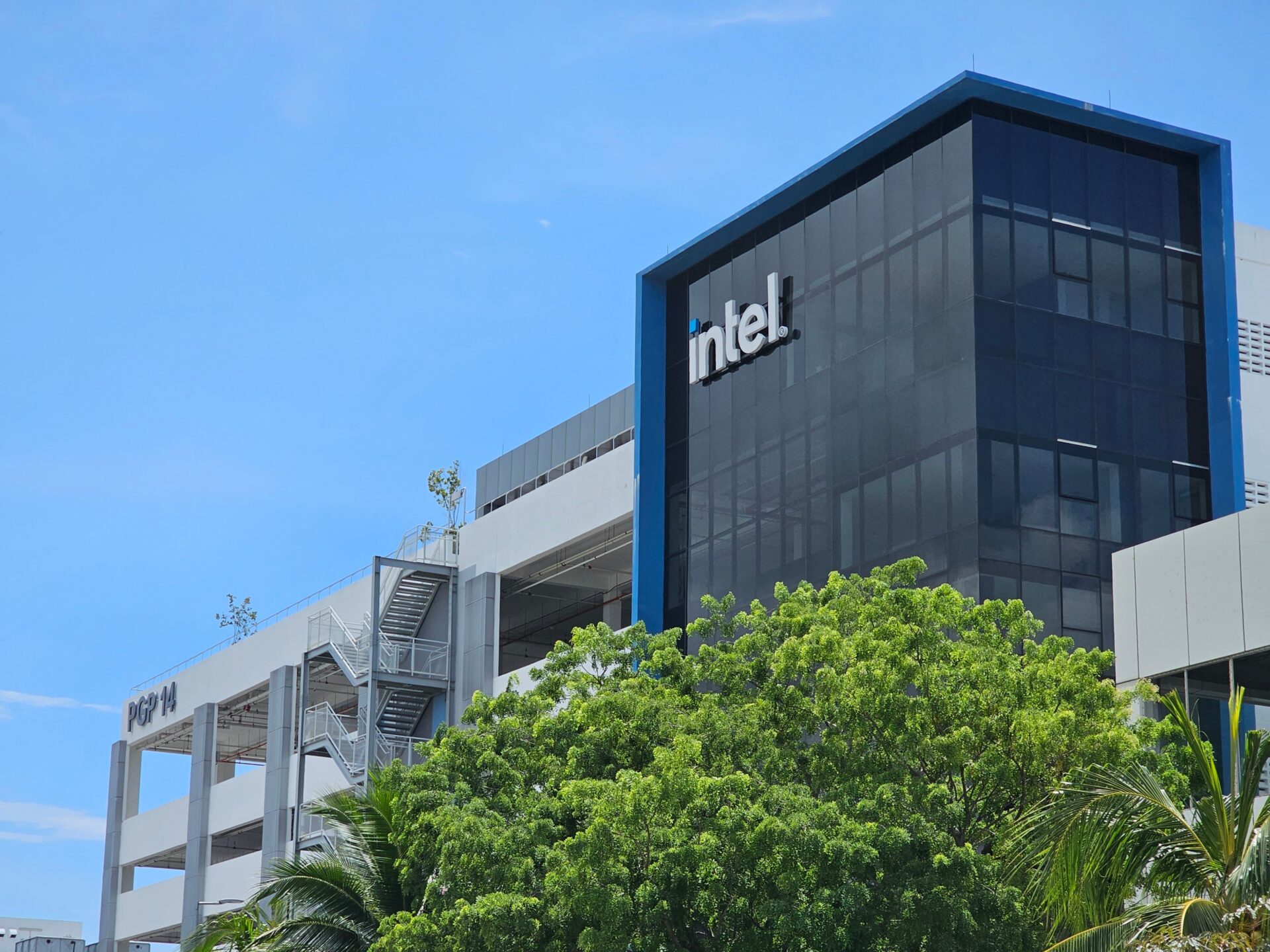
This was the picture executives from the American semiconductor giant sought to paint during a media tour of Intel’s Malaysia operations in Penang and Kulim, Kedah in late-August this year.
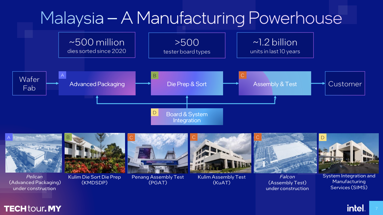
Malaysia is Intel’s first offshore site in 1972, and is today among its largest chip packaging, assembly and test sites outside of the United States.
A quick primer
Chief among Intel’s plans to catch up to foundry rivals Taiwan Semiconductor Manufacturing Company (TSMC) and Samsung Semiconductor is an ambitious plan to execute five process node improvements in four years, and making available its foundries – traditionally reserved for Intel’s own products – to customers such as Qualcomm and MediaTek.
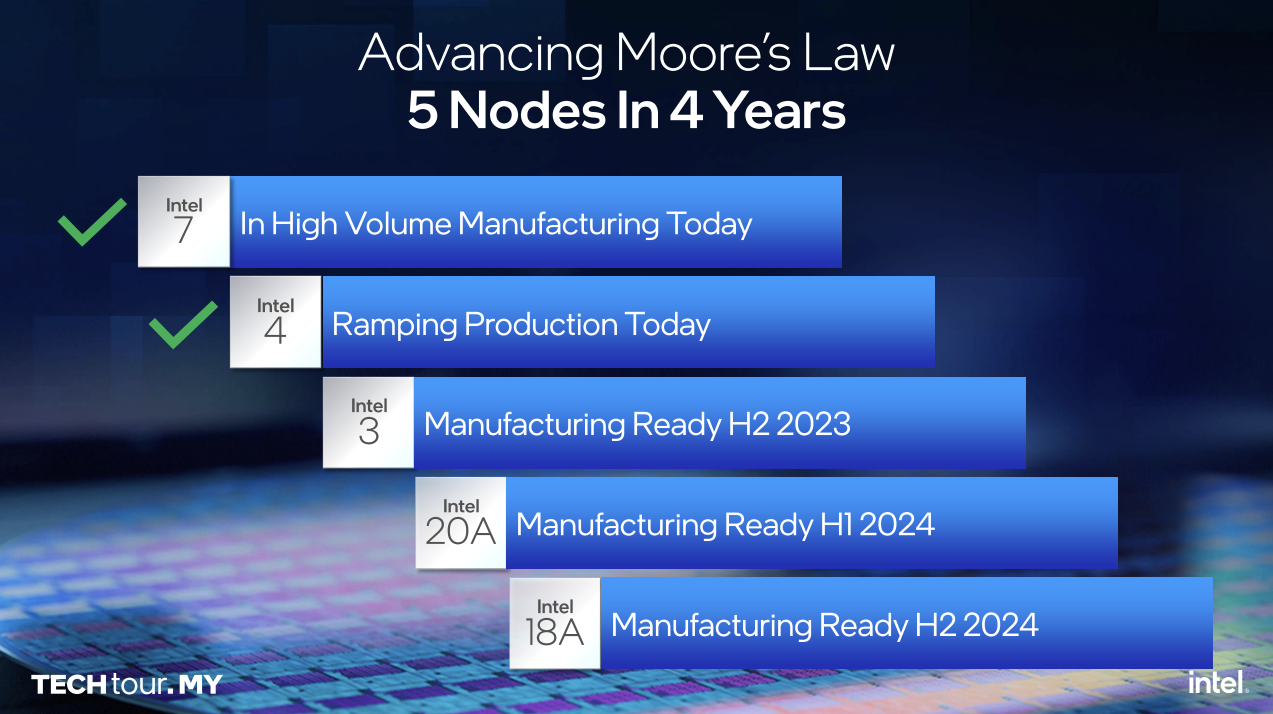
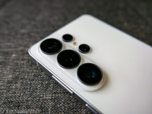
Intel’s 7-nanometer process is already in volume production on its Sapphire Rapids server chips and Raptor Lake PC chips, while its 4-nanometer process is widely expected to debut on the Meteor Lake product in the coming months.
As transistor density improvements become increasingly elusive, Intel and its semiconductor peers are turning to advanced packaging (AP) to squeeze more performance out of its chips.
Instead of designing and accommodating all the processing needs (for instance, for computing, gaming, media consumption, among others) of a product on a singular, monolithic chip, these needs are disaggregated onto individual “tiles” with their own densities and designs, and integrated as a singular chip product through the AP process.
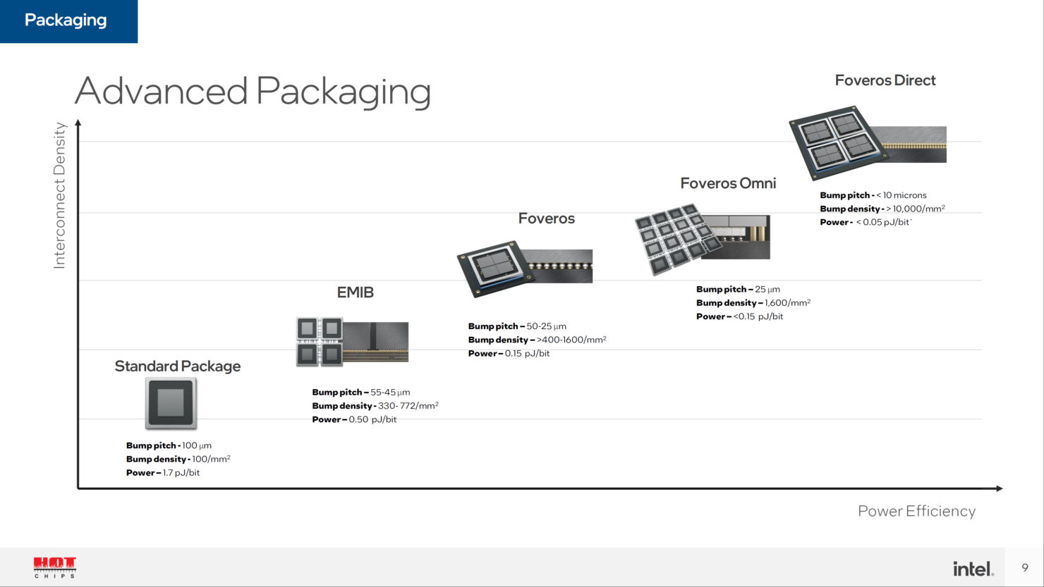
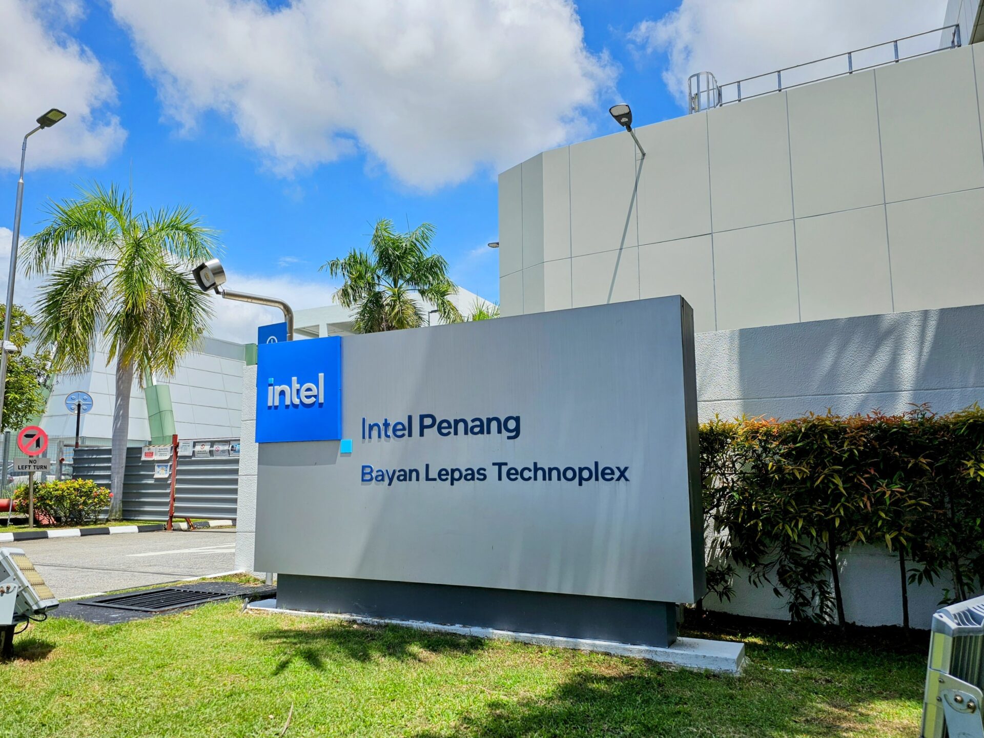
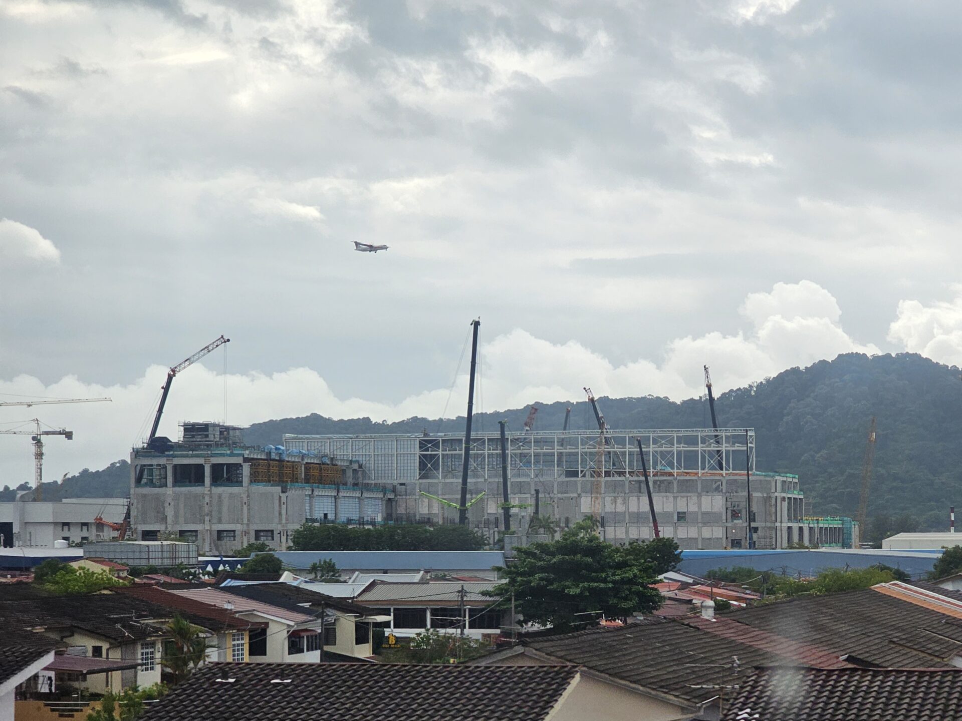
Intel is building its first overseas AP facility (Intel calls its AP process Foveros, for those interested) in Penang, which will also become its largest 3D AP facility once open. This is part of its US$7 billion investment in the country announced in 2021, which also included a third assembly and test facility in the country.
When the AP facility opens, Intel Malaysia will be equipped to undertake a full suite of semiconductor activities except wafer fabrication – its only overseas operation able to do so. This is probably the reason the tour is hosted in Malaysia.
Diving in
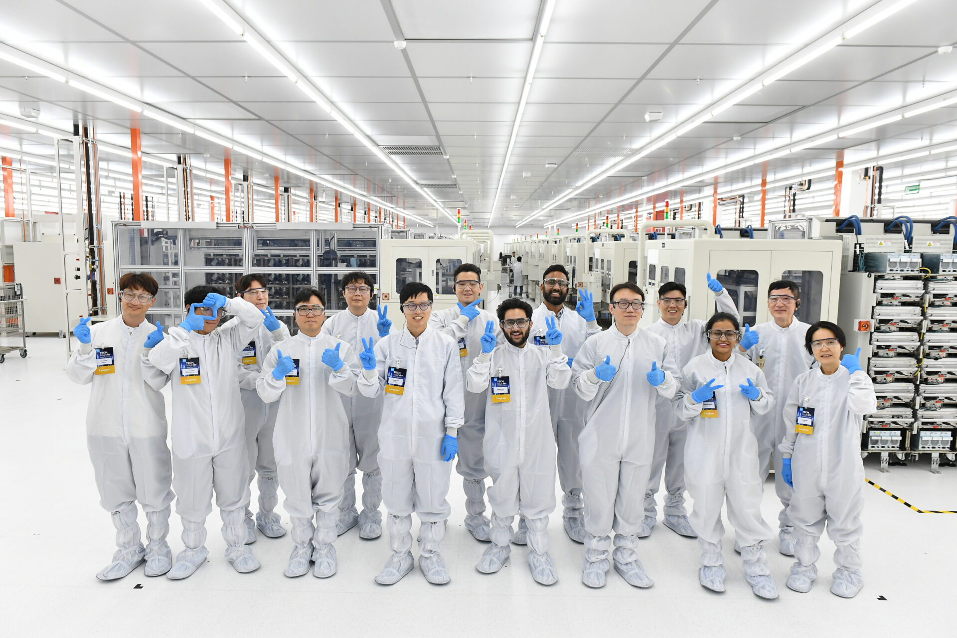
While the new facilities are akan datang (coming soon in Bahasa Melayu parlance), Intel has decided it will not wait any longer to allow the gathered media a peek into the facilities in operation, over a jam-packed two-day field trip.
Reporters were told the parts of factories visited were never seen even by Intel’s own staff unless if they worked there. How could we at Techgoondu resist the opportunity to jump into one of the bunny suits and have a closer look?
(For those curious, it took me five minutes to be suited up, with assistance by a friendly member of Intel staff. I was told employees are normally done in less than half that time, unassisted.)
Security was tighter than at Singapore’s National Day Parade. All electronic devices were surrendered before every tour, and no notebooks allowed. Security personnel wanded us down with metal detectors before and after visiting every factory floor.
Here’s a recollection of the revealing trip inside Intel’s new facilities:
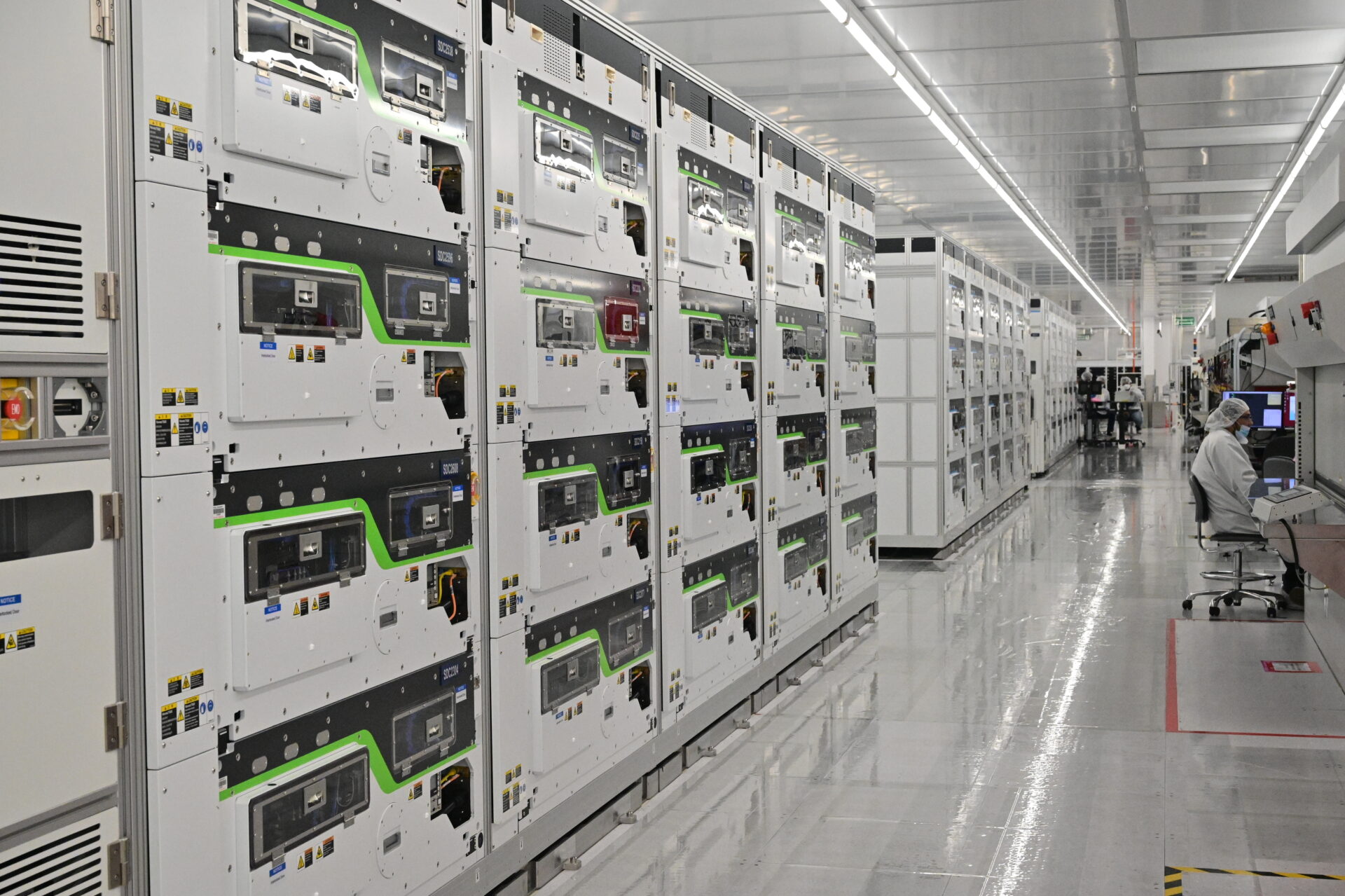
Kulim Die Sort Die Prep (KuDSDP)
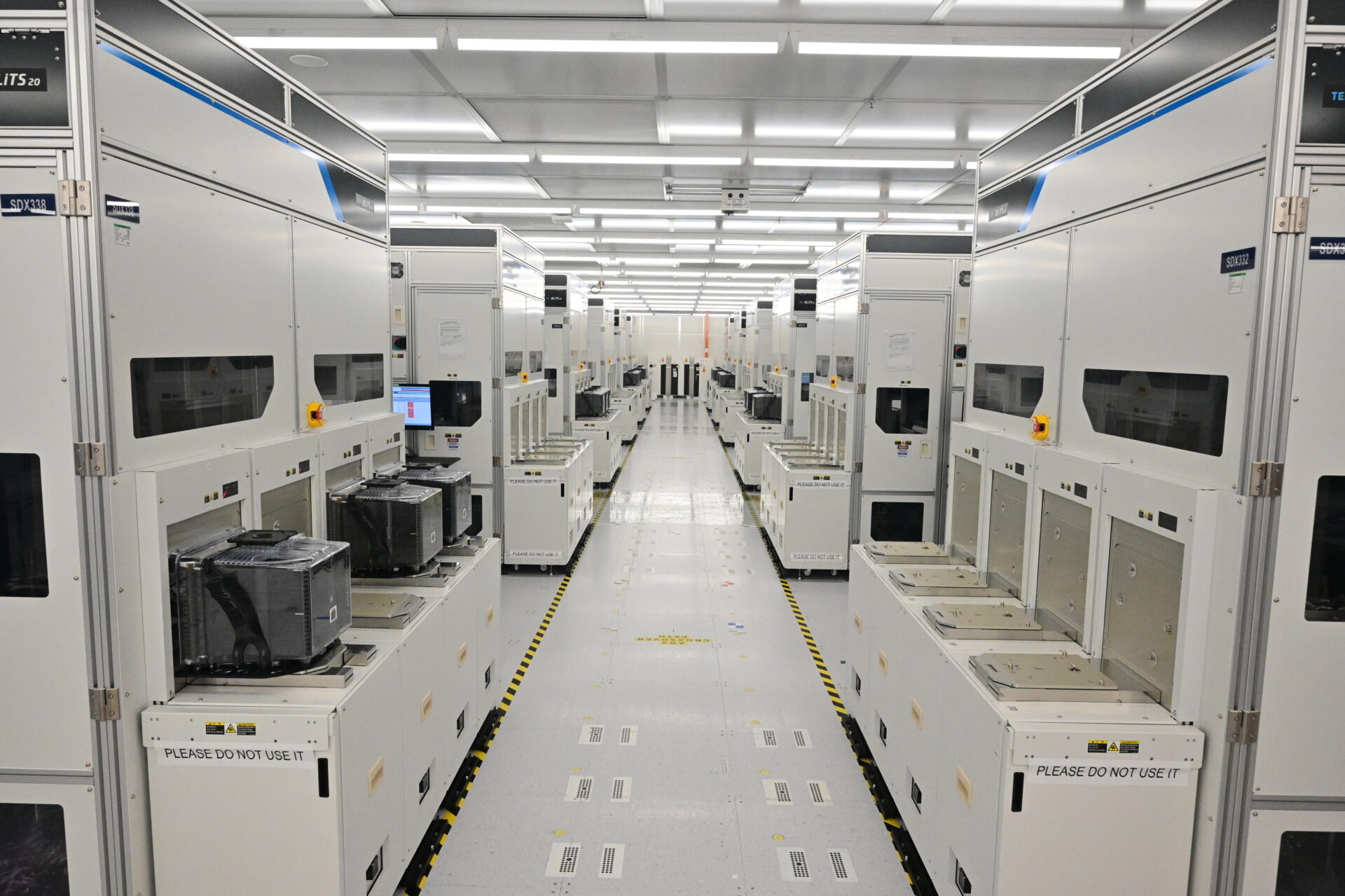
This story starts with KuDSDP, the newest of all Intel Malaysia facilities (thus far). Die Sort went live in the midst of the Covid pandemic in 2021, while Die Prep was only partially commissioned when we visited – the latter opened in Q3 2022, and parts of the shop floor awaited the arrival of equipment.
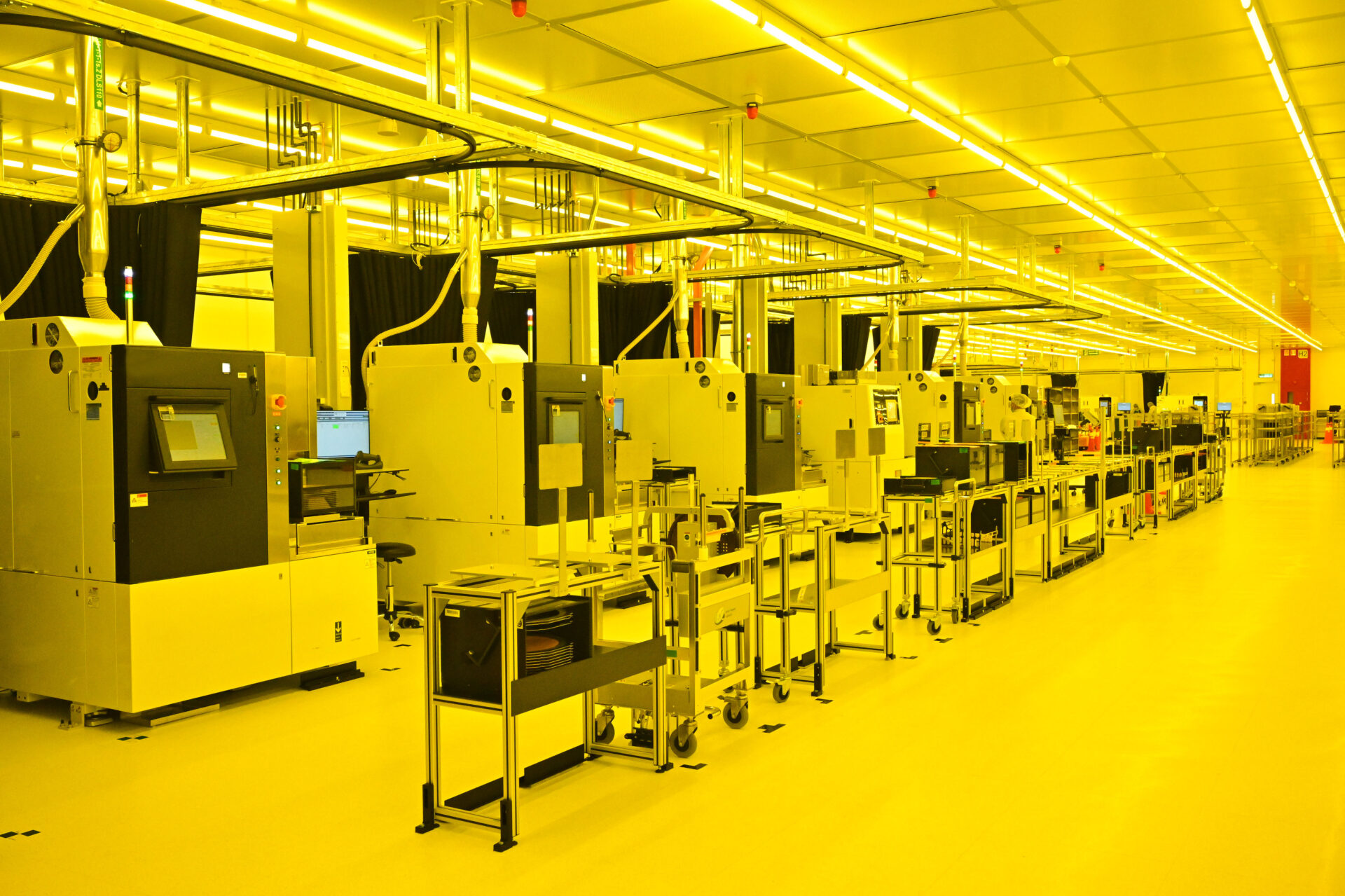
We began the visit with Die Prep, where a silicon wafer is cut into individual chips (called dies) through grinding, laser scribe, and/or mechanical cutting by precision machinery.
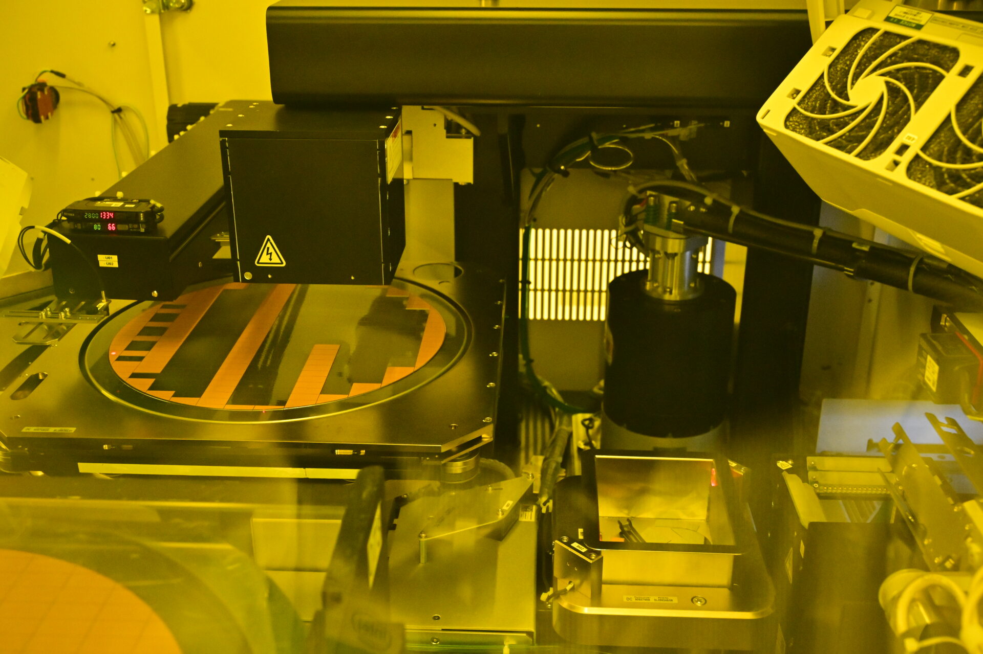
The entire space was bathed in yellow light. I was told this was necessary, as the transfer media on which the cut dies were transported would react with ultraviolet rays and turn sticky otherwise.
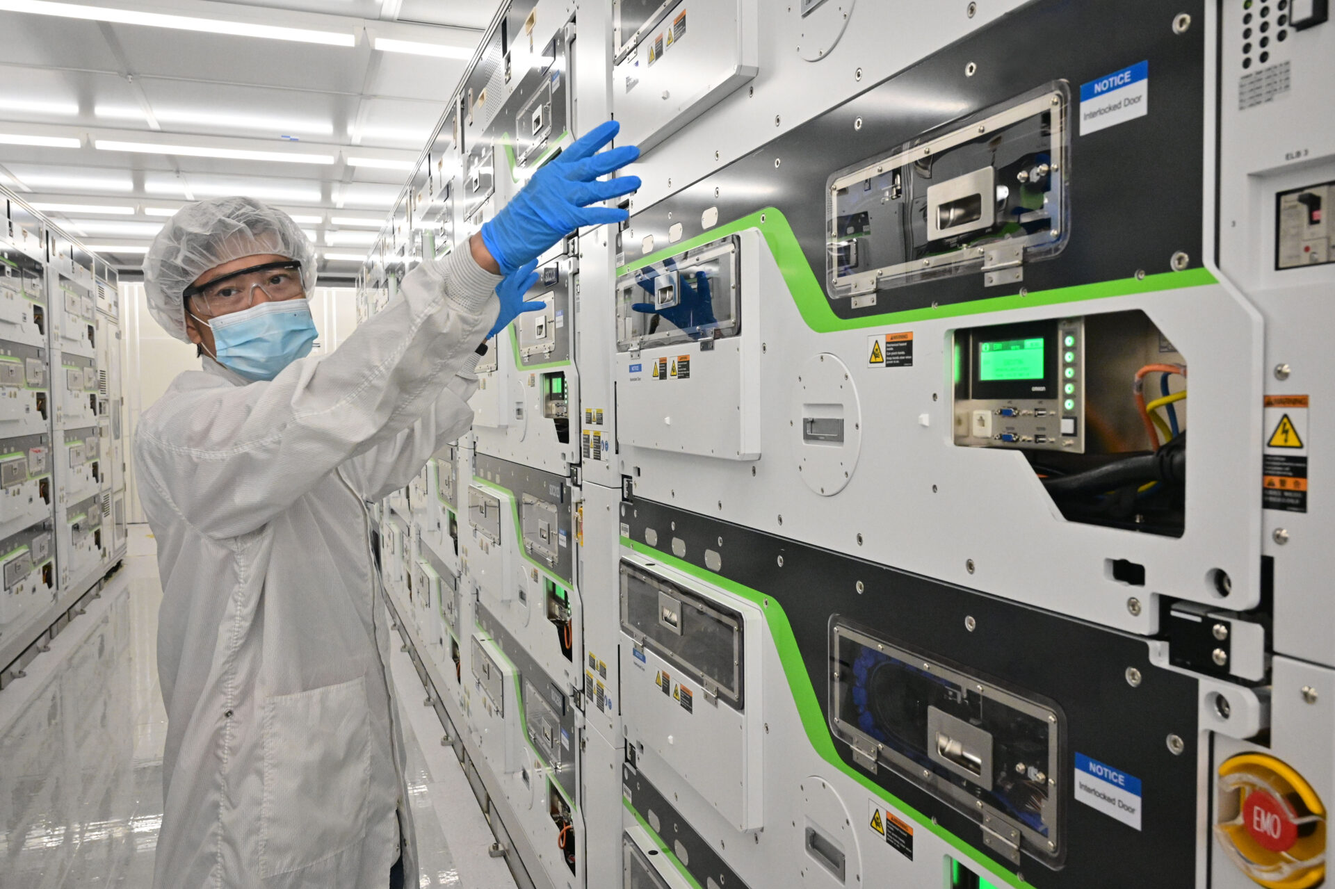
Next, Die Sort is when chips are tested for defects and its performance measured. A chip may, say, be graded as a standard product, or a K product suited for overclocking to squeeze out extra performance.
To achieve this, every chip is tested by a sort module made up of 20 individual test cells. Each chip is tested on a probe card which contains thousands of fine needles thinner than a human hair, connecting to the integrated circuit inside the test equipment. It measures the electricity of the chip circuits for reliability and defect analysis.
The factory line managers hosting us were coy to confirm the full details, but their presentation slides indicated known good die yields from Intel’s die sort for disaggregated chips could be nearly 10 per cent higher than competition.
Each test cell weighs about 1,000 pounds and is moved around by a custom design lifter mechanism. In practice, it looks like a massive transparent cage, which floats on the cushion of air like hovercraft. This prevents damage to the factory floor.
During the tour, two petite women were able to move the lifter with relative ease. While I was not able to get pictures, the air cushion transporter concept truly seemed like it came straight out of a sci-fi movie.
Finally, the same grade of dies will be packaged into tape reels that look like very large rolls of black masking tape.
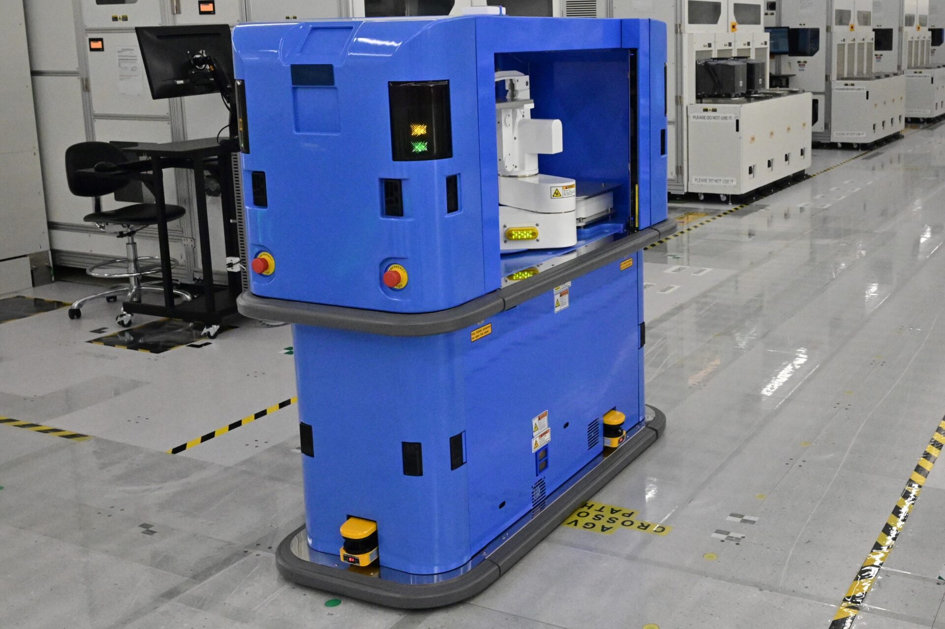
As a new factory, there is automation to keep cycle time to an absolute minimum, including customised autonomous robots able to draw and deliver trays of dies between storage holds, and the die prep and die sort machines.
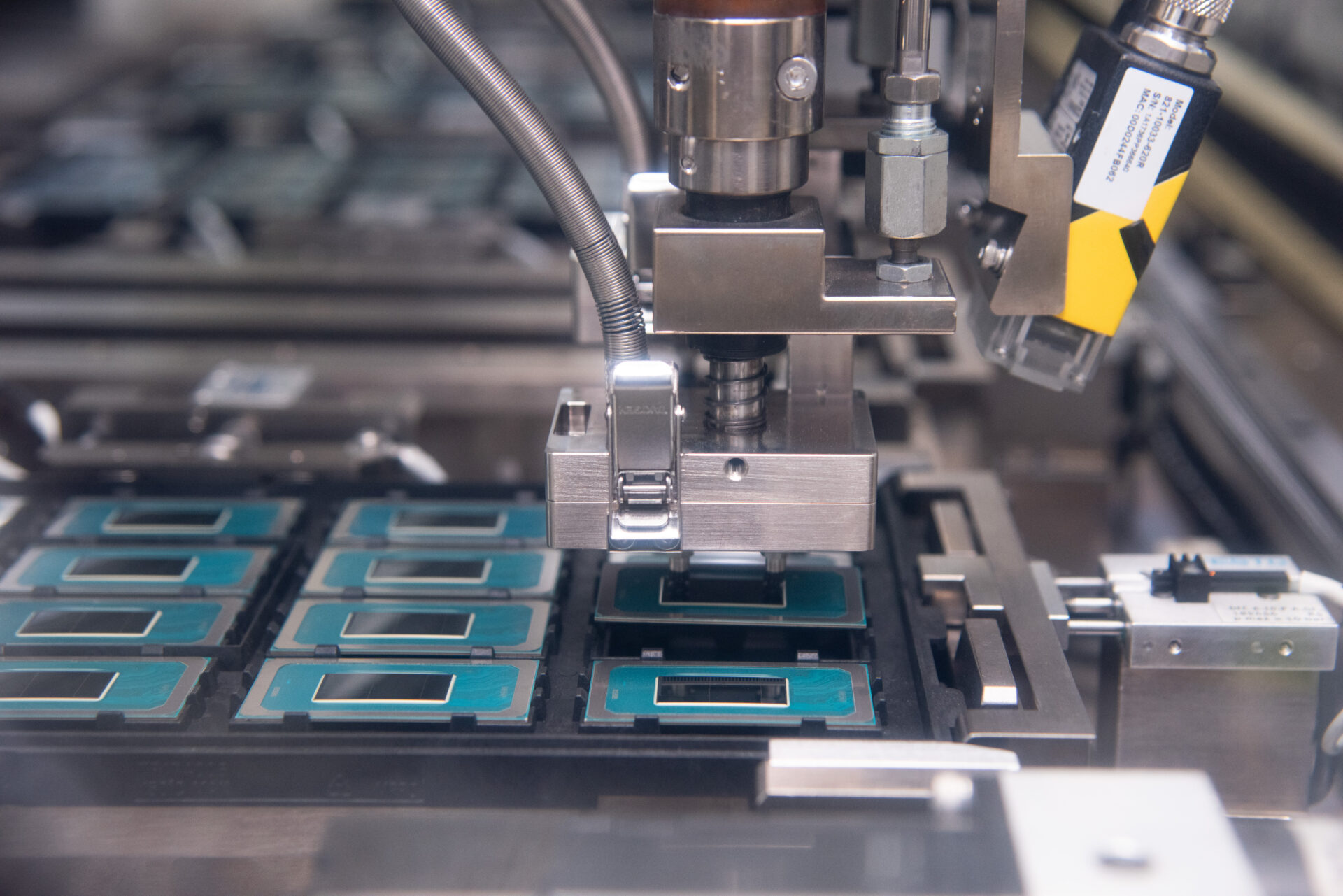
Penang Assembly and Test (PGAT)
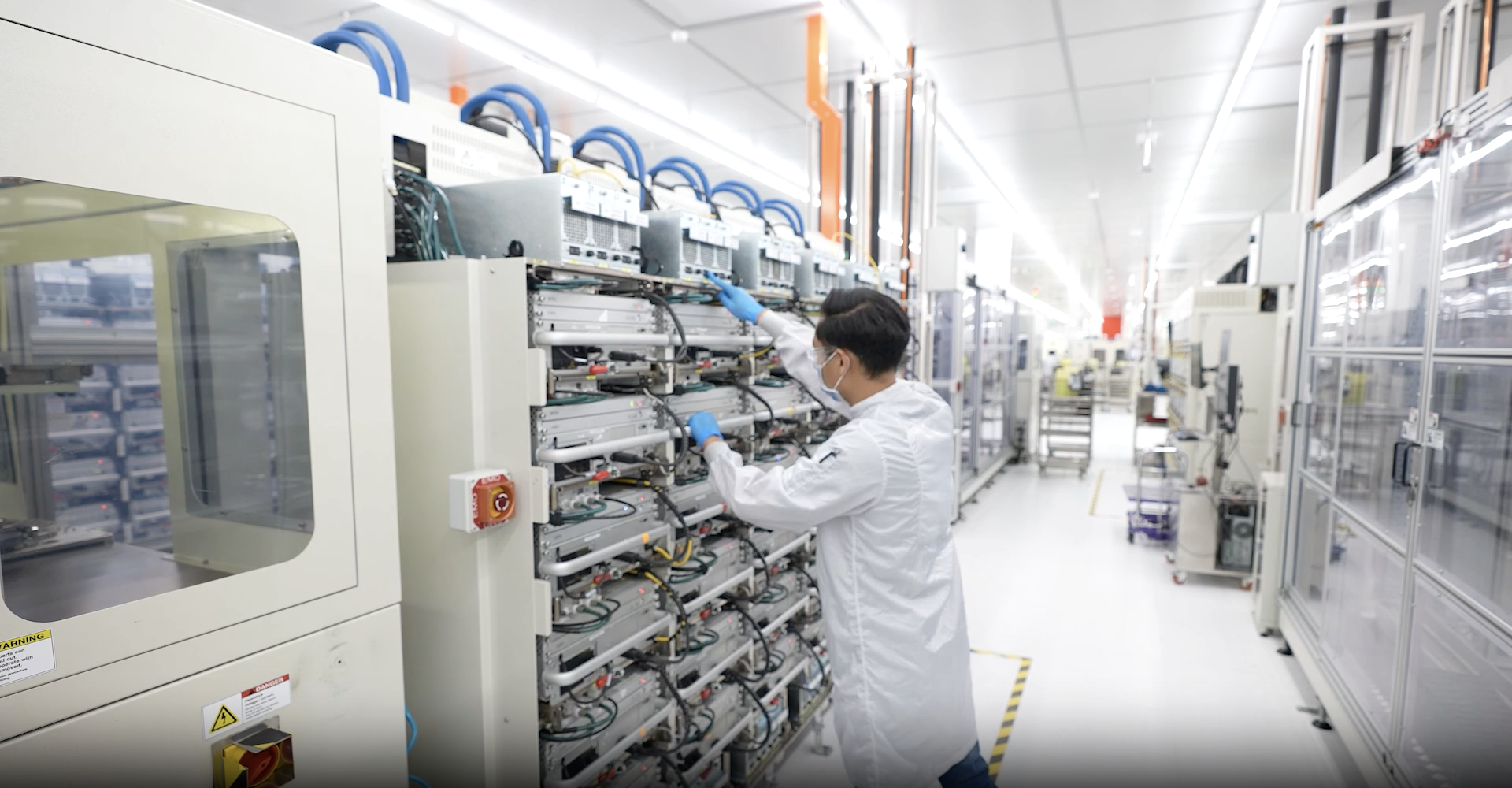
Assembly and Test is the mainstay of Intel’s Malaysia operations, spread over its Penang and Kulim AT sites, with a third coming online in time to come. We visited the former.
Here, silicon dies supplied by global Intel die sort facilities (including KuDSDP) are mounted onto PCB substrates and epoxied, before a heat spreader is attached to become familiar Intel Core and Xeon processors (among others). Assembled chips are put through temperature, stress, performance, and quality tests before being sent to customers.
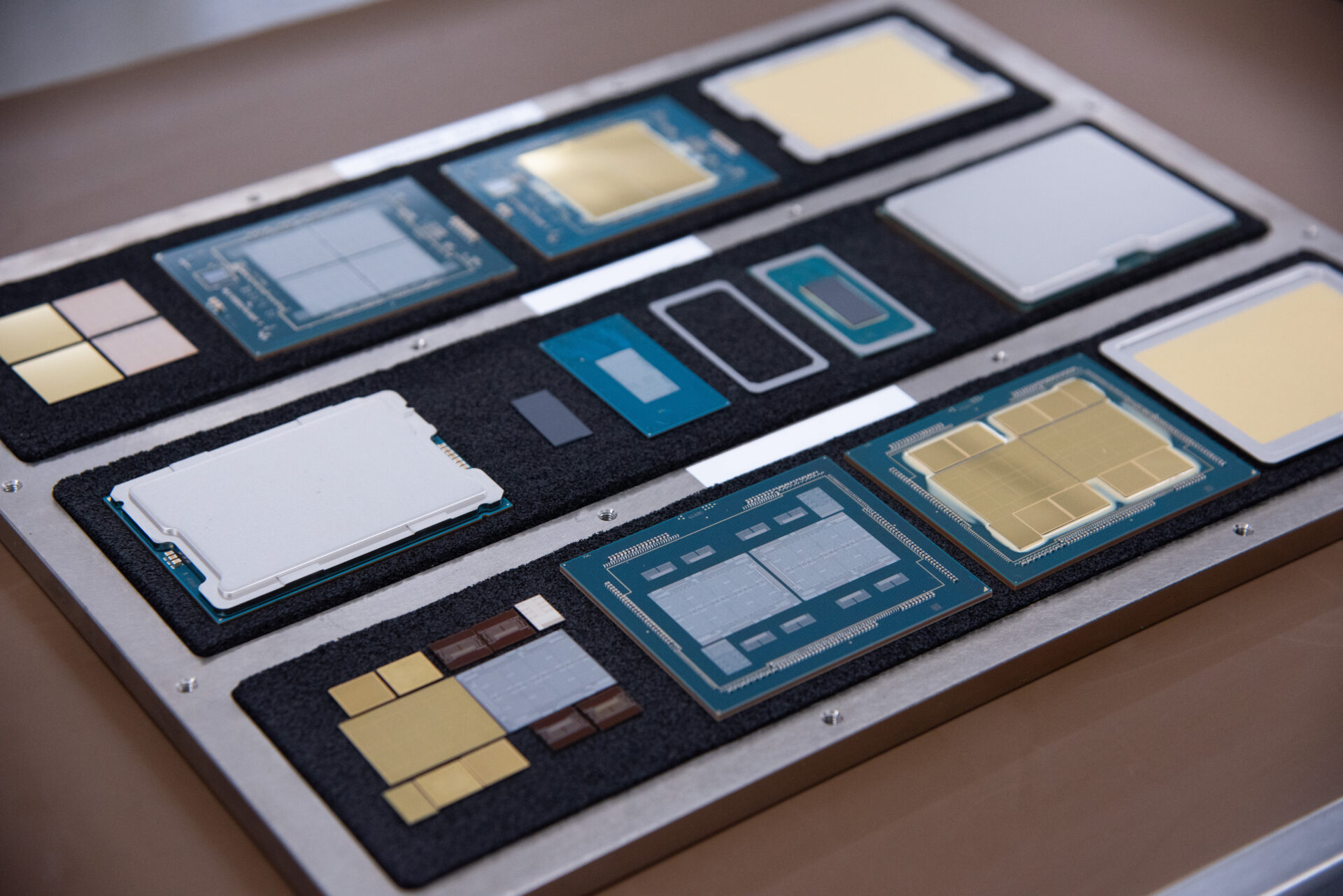
Chip Attach is the first step, starting from the silicon dies that arrive at PGAT mounted on tape reels. The dies (the grey or gold chips on a black reel) are separated from the reel, and attached to a PCB substrate (the green board) alongside other components.
Next, the substrate with the newly attached die and components has epoxy material applied to ensure stress is uniformly distributed across the die. No pictures unfortunately, but the precision with which the machines analyse, then inject just the right amount of epoxy to fill the gaps is astounding.
Lid Attach follows, where thermal conductivity paste is applied to the die before a metallic heat spreader is added.
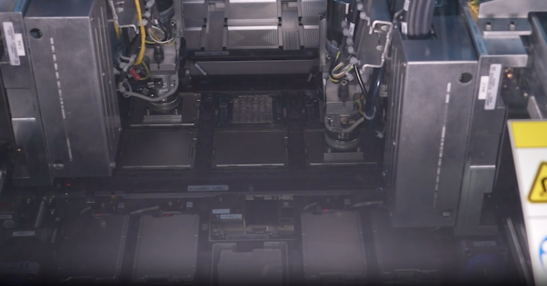
The end product is a CPU or a processor with the circuit enclosed in a metallic lid. Once a finished CPU rolls out of the lid attach process, they are loaded onto trays for Burn-In, stressed at high temperatures and voltage to screen out defects.
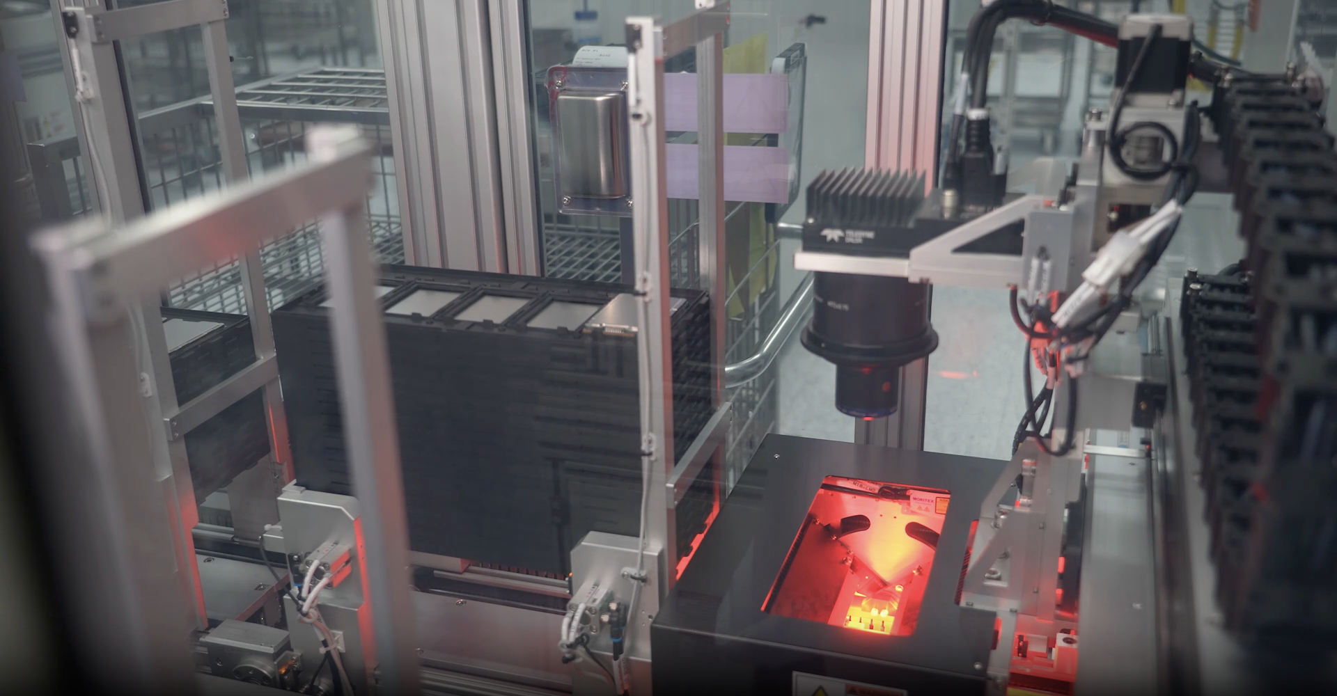
Following burn-in, a series of electrical tests are performed to ensure only functional devices are shipped to customers. This includes testing of all electrical traces as well as functionality.
The final test, PPV, mimics customer end-product test conditions and platforms. Devices are mounted onto a testing environment that conforms to specific test conditions, platforms, and operating systems.
Concluding thoughts
Throughout our visits, we were consistently hosted and briefed by very many senior Malaysian staff, nearly all of whom has spent nearly two decades with Intel Malaysia.
From their knowledge and enthusiasm in responding to our queries, the collective ownership over Intel’s vision and commitment to knowledge transfer is palpable, at least in my short time spent with them.
Look out for more reports from our visit to Intel’s Malaysia facilties soon.