In association with Keysight Technologies
By Choon-Hin Chang
Printed circuit board assembly (PCBA) manufacturers rely on in-circuit test (ICT) systems to detect manufacturing processes and component defects. Manufacturers prefer ICT systems for testing electronic assemblies because they are easy to programme, have extensive fault coverage, rapid test throughput, low false fail rates, and outstanding diagnostic accuracy.
In recent years, the landscape of ICT systems has undergone a significant transformation, driven by advancements in PCBA technologies, evolving test philosophies, and shifting manufacturing business models. These changes have created an array of new and diverse requirements for ICT manufacturers to accommodate.
The challenges include diminishing test point access in specific product sectors, with a growing threat from the increase in low-voltage differential signaling integrated circuits used for high-speed signaling and ball grid array devices. These complexities motivate ICT manufacturers to innovate and adapt, preserving the effectiveness and relevance of their testing solutions.
In this article, we explore the latest advancements in ICT that are revolutionising manufacturing tests by increasing coverage, reliability, and throughput in in-circuit production tests, ultimately driving down costs.
The introduction of ICT systems
The introduction of ICT systems in the late 1970s marked a milestone in electronics manufacturing. The landscape at that time was vastly different from today’s. PCBAs used through-hole technology, and components sat on a single side of the board. The prevailing voltages powering these boards were typically no more than 15 volts. During this era, functional tests for manufacturing were complex and time-consuming.
Precision and efficiency are essential in electronics manufacturing. As technology advances and consumer demands evolve, rigorous testing methodologies are becoming increasingly crucial.
Among these methodologies, ICT stands out as a way to ensure the quality and reliability of PCBAs. The advent of ICT systems transformed PCBA manufacturing. The process shifted from assessing the board’s functionality to evaluating the functionality of individual parts and ensuring the integrity of the assembly process.
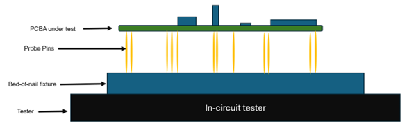
ICT systems assess the board’s functionality by employing a bed-of-nails test fixture, as shown in Figure 1. In a bed-of-nails test fixture consisting of spring-loaded pins, the pin positions align with the PCBA’s test point. When the tester places the PCBA under test on the bed and presses down, the pins make electrical contact with test points or component leads on the PCBA.
These contacts enable the tester to inject signals and power at specific points on the PCBA while measuring electrical properties and responses, such as resistance, capacitance, inductance, and voltage levels.
With robust electrical test access and innovative guarding and voltage-forcing techniques, each component can undergo individual testing. These readings help verify component connections and check for manufacturing defects like open circuits, short circuits, or incorrect component values. The underlying principle is that manufacturers can trust the board’s functionality if ICT verifies the correct operation of all components and ensures proper assembly.
Navigating the complexity of testing diversity
As technology advances, printed circuit boards (PCBs) are getting smaller and more complex, making it harder to ensure full electrical test access. Low-voltage differential signaling integrated circuits used for high-speed differential signaling, increased use of ball grid array (BGA) devices, and faster input/output speeds are contributing to this challenge.
To accommodate this trend, manufacturers are crafting intricate high-density interconnect boards featuring concealed and buried vias, narrower tracks with tighter spacing, and reduced copper availability on the board surface for electrical test access.
Manufacturers of ICT systems have not only addressed the technological needs but also adapted to align with changing testing philosophies and business drivers. ICT vendors have encountered challenges in meeting the diverse needs of various manufacturers, each of whom specifies unique requirements for its ICT system and holds distinct expectations regarding system functionality.
For instance, low-margin manufacturers prioritise cost-effective ICT solutions. Manufacturers producing reliable, intricate products require comprehensive fault coverage and extensive pin count capacity. High-volume manufacturers demand increased test throughput and manufacturers employing outsourcing models seek equipment compatibility.
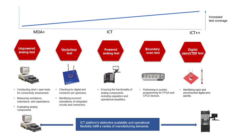
Over time, ICT vendors have addressed conflicting demands by providing varied tiers of ICT systems. Figure 2 illustrates the strategy that empowers manufacturers to precisely procure the required test capabilities, allowing for scalable adjustments without necessitating changes to the tester.
However, if the manufacturer operates only a manufacturing defect analyser (MDA+) class tester, it may struggle to test complex PCBAs because of limited capabilities. Conversely, choosing a high-performance ICT platform could be excessive for simple PCB assemblies, where advanced features are unnecessary and programme development demands highly skilled operators.
Enhancing test coverage
When the TestJet technique was introduced in the 1990s, it was a real breakthrough for increasing coverage of in-circuit tests. But today’s PCBAs are inadequately covered by capacitive probe measurement techniques, including TestJet, opening the door to Vectorless Test Enhanced Probe (VTEP) technology.
Vectorless technology
The use of VTEP improved ICT coverage, especially on boards with hard-to-test packages such as BGAs, micro-BGAs, and SMT edge connectors. Today’s nanoVTEP technology provides faster test throughput, essential for high-volume manufacturing, and lower-cost fixtures. Finally, the higher fault coverage of nanoVTEP enables reliable and efficient solutions for PCBA testing.
Boundary scan test
As technology evolves, complex interconnects, limited access points, and increasing component density make chipset testing more challenging. For instance, densely populated server boards with higher clocking frequencies require additional design considerations to preserve signal integrity and minimise undesirable distortion. Close-running parallel traces may generate electromagnetic interference, while test pads on a high-speed path may result in reflections and signal degradation.
PCBAs have low ICT coverage because of limited electrical access. A boundary scan test enables a manufacturer to check a PCBA’s functionality without having full access to its internal circuitry to ensure accurate and reliable testing.
The prerequisite is that the manufacturer needs to design the PCBA according to the IEEE 1149.1 standard, which requires boundary test cells connected to each pin. Using IEEE 1149.1 standard information, the manufacturer can easily verify the overall functionality of a PCBA without needing to check on its components.
Optimising test efficiency in high-volume manufacturing environments
In high-volume manufacturing environments, the efficient and reliable production of a PCBA is crucial to meeting market demands and maintaining competitiveness. With assembly equipment speeds surging and beat rates now often measured in seconds, the in-circuit tester risks becoming the bottleneck.
This situation presents a dilemma for manufacturers: either expand test capacity by adding more equipment or reduce test durations to align with the target beat rate. Both options present challenges.
Adding more equipment is costly, demands additional fixtures, and may not be feasible because of spatial constraints in production facilities. Conversely, trimming tests necessitates extra programme maintenance and diminishes the ICT system’s ability to detect defects effectively.
A better approach is to increase the tester’s execution speed until it is no longer the bottleneck on the production line. Some ICT systems have evolved to support concurrent testing of more than one component. This process involves duplicating instrumentation in the test system so that the test executive can test multiple components in parallel, typically on boards manufactured as part of a panel.
In traditional setups, in-circuit testers typically limit testing to up to four boards at a time. However, high-volume manufacturing environments, where efficiency and throughput are critical, demand the ability to test a larger number of boards simultaneously.
Massively parallel board testing can test multiple boards at the same time using multiple testing cores. By implementing parallel testing, where we assess multiple units simultaneously, we reduce the time needed to test each unit. This advancement significantly boosts testing throughput and efficiency across the board, optimising the testing process.
Conclusion
Over time, ICT systems have undergone significant evolution to tackle the technological and business hurdles of contemporary PCB manufacturing. Their functionalities have expanded considerably since their inception.
Enhanced methodologies like reduced access testing, integration of boundary scan, nanoVTEP technologies, embedded testability tools, parallel testing abilities, functional testing capabilities, and adaptable system configurations have prolonged the relevance and utility of ICT systems.
Consequently, ICT remains one of the primary tools that high-volume PCBA manufacturers use to identify defects in manufacturing processes and components.
Choon-Hin Chang is product marketing manager at Keysight Technologies. Chang has 30 years of experience in project management and engineering leading new product introductions as well as business, manufacturing, process improvement, supply chain management, strategic sourcing, and operations.