Singapore’s Agency for Science, Technology and Research (A*Star) has inked a deal with chipmaker GlobalFoundries (GF) to explore how to better package semiconductors to boost performance, as the traditional way of shrinking and packing in more transistors becomes increasingly difficult.
Today’s advanced packaging combines several chips (or chiplets) into one unit to improve performance, lower power use, and create smaller designs. This is key for technologies like artificial intelligence (AI), high-performance computing, data centres, and future networks such as 5G and 6G.
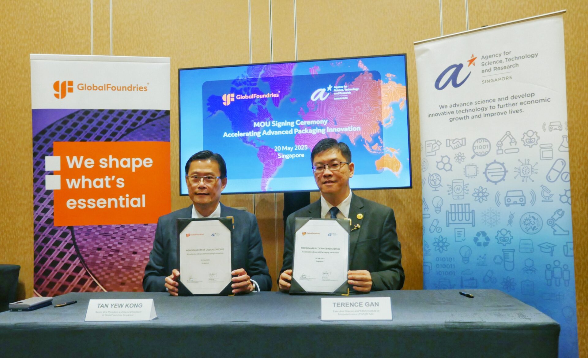
With the partnership, GF will have access to the research and development facilities, capabilities, and technical expertise of A*Star, Singapore’s public-sector research and development agency.
In return, GF will provide A*Star with equipment for the research. The partnership includes initiatives to upskill GF employees in advanced packaging technologies.
GF aims to enhance its advanced packaging capabilities and provide a range of services – encompassing chip fabrication, packaging, and testing – at its Singapore manufacturing facility.
Singapore’s robust semiconductor ecosystem and strong R&D support from the government and institutions like A*Star makes it an ideal location for GF to develop and scale its foundry-level innovations, said Gregg Bartlett, GF’s chief technology officer.
“This aligns to our global advanced packaging roadmap and reinforces our commitment to deliver more energy-efficient essential chips that are crucial for our customers, especially in the AI era,” he added.
Terence Gan, executive director at the A*Star Institute of Microelectronics, said: “As Singapore strengthens its position as a critical node in the global semiconductor supply chain, continued R&D collaboration between public research and the industry is essential to drive innovation and maintain our competitive edge.”
Earlier this year, GF announced plans to create a new advanced packaging and photonics centre for advanced packaging and testing of American-made “essential” chips within its New York manufacturing facility.
The advanced packaging market is set to grow at a compound rate of 5.70 per cent a year, according to Research and Markets. The market was valued at US$39.60 billion in 2024, and is expected to grow to US$55 billion by 2030.